Disclosure: Bridgetek provided the IDK-BT817-70A kit used in this tutorial free of charge with no obligations. Bridgetek did not fund this tutorial nor did they review or approve its content, and every setting, problem and result described here comes from my own bench.
Why this kit? I was looking for a display to pair with QSPI. The NUCLEO-H753ZI was already my QSPI board from the W25Q flash tutorial, and after the RA8875 tutorials I wanted to try a display controller that works differently. The Bridgetek BT817 fit both.
Overview
This tutorial sets up the Bridgetek BT817 IDK-BT817-70A development kit and puts a first screen on its 7-inch touch panel with EVE Screen Designer, straight from a Windows PC over USB. There is no STM32 in this part: before writing a single line of firmware, it pays to see the kit work with the vendor’s own tools, so that every later problem can be blamed on the firmware and not on a cable or a switch.
The Bridgetek BT817 is an EVE (Embedded Video Engine) graphics controller of the fourth generation. Unlike the RA8875 used earlier on this site, which keeps a framebuffer that the microcontroller draws into pixel by pixel, the BT817 is driven by a display list: the host sends short commands (“draw this text”, “draw a button here”, “show this image from flash”) and the BT817 renders the whole screen by itself, every frame. It also reads the capacitive touch controller, calibrates the touch screen on its own, drives a speaker, and keeps images and fonts in its own 16 MB flash. The host only needs an SPI or QSPI port, which is why it fits small microcontrollers so well.
This is Part 1 of a series. Future posts will connect the same kit to a NUCLEO-H753ZI, first over plain SPI and then over QSPI. Along the way this part covers the things that cost me time on the bench: the connector labels, the switch and jumper settings, a touch cable that has to go in differently from the kit datasheet, and a calibration screen that looks like the kit has hung.
Related tutorials: STM32 RA8875 Library: 7-Inch TFT LCD on NUCLEO-F439ZI drives a 7-inch panel through a framebuffer controller, and STM32 FRAM Touch Calibration with RA8875 and MB85RS64V does the touch calibration math in our own code, which the Bridgetek BT817 does for you.
What You Will Learn
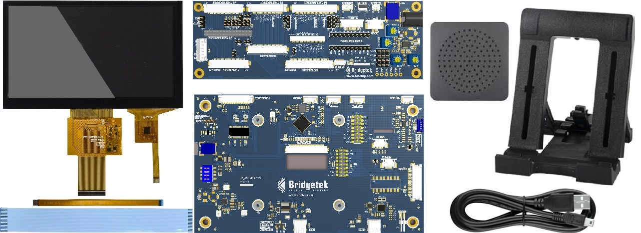
- What is in the IDK-BT817-70A kit and what each board does
- How to read the two labels printed next to every connector on the Bridgetek BT817 boards
- The switch and jumper settings for running the Bridgetek BT817 kit from a PC over USB
- How to connect the display, the ribbon cable and the touch cable, including the orientation that actually works
- How to install EVE Screen Designer, build a first project and run it on the hardware, not the emulator
- What the touch calibration screen looks like, and how the BT817 stores the result
Prerequisites
No programming is needed for this part. You need a Windows 10 or Windows 11 PC (EVE Screen Designer is a Windows program; I ran it in a Windows 11 virtual machine on Linux, and the notes for that setup are in the installation section), a free USB port, and some care with small flat cables and their latches.
Materials List
Everything comes in the Bridgetek BT817 kit, IDK-BT817-70A:
| Part | What it is |
|---|---|
| ME817EV | The main board: the BT817 controller, a 16 MB NOR flash for images and fonts, an FT4222H USB-to-QSPI bridge for the PC, an audio amplifier, and the CN8 host header used later with the STM32 |
| VA-1001-01A | The LCD adaptor: it takes the panel signals from the ME817EV over the 50-pin ribbon and supplies the panel with the right voltages |
| DP-0701-01A | The 7-inch 800 x 480 RGB TFT panel with an FT5426 capacitive touch controller on its own 10-pin flex |
| 50-pin ribbon cable | Joins the ME817EV to the VA-1001-01A |
| 10-pin extension cable | Carries the touch signals from the panel to the ME817EV |
| USB-A to USB-C cable (1 m) | Power and data from the PC |
| CleO speaker (8 ohm, 1 W) | In its own small enclosure, for the audio output |
| LCD stand | Holds the panel upright on the bench |
Bridgetek’s own kit list in the EVE IC Development Kits datasheet (section 3.3, linked under Documentation below) names seven items. It counts the adapter and its cables as one “universal LCD adapter package”, which is why the table above has eight rows.
Bridgetek BT817 Board Diagram
There is no Nucleo board in this part, so instead of a pinout page this section maps the two boards of the Bridgetek BT817 kit: the ME817EV, which carries the BT817 itself, and the VA-1001-01A adapter, which feeds the panel.
Every connector on these boards carries two labels: a reference designator such as CN10, which is what the datasheets and schematics use, and a short function label such as MT_CTP10. This post always gives both, for a good reason: the two boards reuse the same designators. The ME817EV has a CN10 for touch and the adapter has a CN10 for a resistive touch panel, and they have nothing to do with each other.
ME817EV
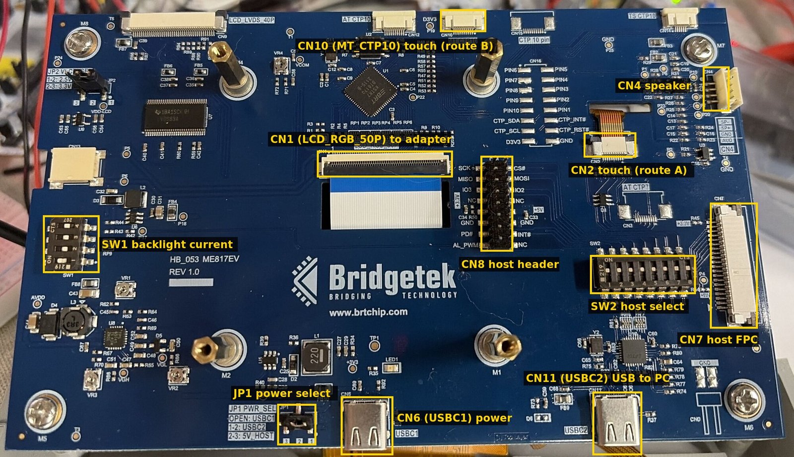
| Designator | Silkscreen label | Purpose |
|---|---|---|
| CN1 | LCD_RGB_50P | 50-pin ribbon to the adapter (RGB signals for the panel) |
| CN2 | (none) | Touch, route A: the panel’s touch cable through the 10-pin extension |
| CN10 | MT_CTP10 | Touch, route B: the short white cable from the adapter’s CN9 |
| CN4 | SP-, SP+, GND, AUD | Speaker |
| CN6 | USBC1 | USB-C, power only |
| CN11 | USBC2 | USB-C, power and USB data to the PC (FT4222H bridge) |
| CN8 | (none) | 2 x 8 host header for a microcontroller (used with an STM32 in future posts) |
| CN7 | (none) | 20-pin FPC version of the host header (not used in this series) |
| SW1 | (none) | Backlight current |
| SW2 | (none) | Connects the BT817 host lines to the FT4222H (PC) or to CN7/CN8 (microcontroller) |
| JP1 | PWR_SEL | Power source: open = CN6, 1-2 = CN11, 2-3 = 5V_HOST from CN8 |
VA-1001-01A adapter
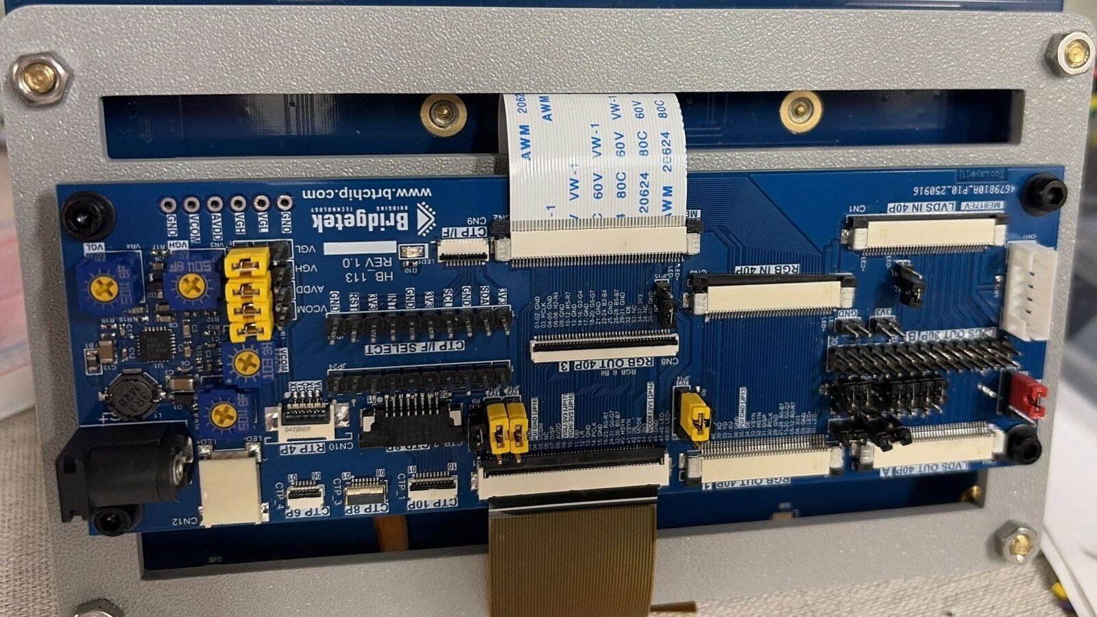
| Designator | Silkscreen label | Purpose |
|---|---|---|
| CN2 | (none) | 50-pin input from the ME817EV’s CN1 |
| CN7 | RGB output 2 | 50-pin output to the DP-0701-01A panel |
| JP14, JP16, JP17 | (none) | Panel voltages: set to 3.3 V for this panel |
| CTP_1 | CTP 10P | Touch, route B: the panel’s touch cable through the 10-pin extension |
| JP24 | JP24 | Touch, route B: one end of the seven jumper wires |
| JP23 | CTP I/F SELECT | Touch, route B: the other end of the jumper wires |
| CN9 | CTP I/F | Touch, route B: short white cable to the ME817EV’s CN10 |
The other connectors on the adapter (the 40-pin RGB outputs, CTP 8P, CTP 6P and RTP 4P) are for other Bridgetek panels and are not used with this kit.
Project Structure
This part has no STM32 code. The “project” is the EVE Screen Designer project, and ESD writes all the C code from it. Here is the project folder after a build. I named my project NewProject4. Yours will carry whatever name you give it:
NewProject4/
├── NewProject4.esd              The project file: open this in EVE Screen Designer
├── App.main                     The application: Start, Update, Render, Idle and End, plus the default theme
├── AppScreen.page               The top-level screen: holds the main page and switches between pages
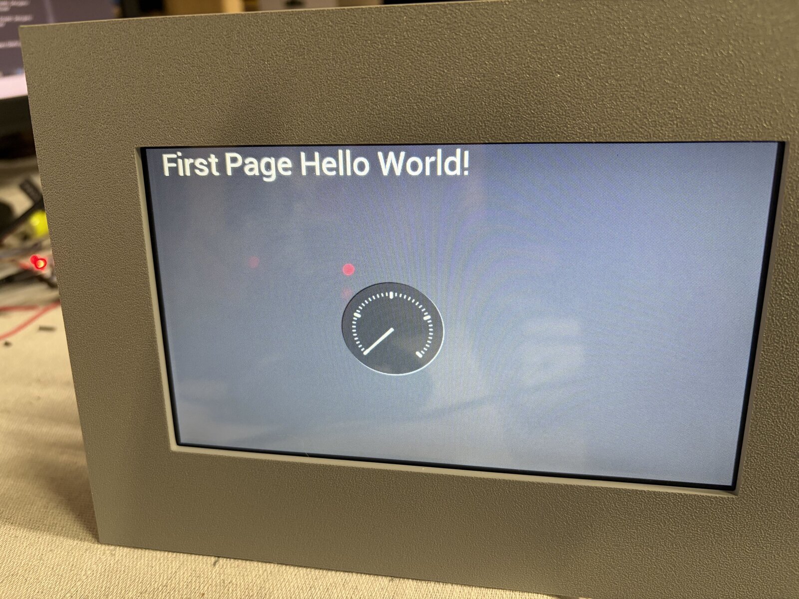
├── FirstPage.page               The page shown on the panel: a Fixed Position layout with a label and a gauge
├── Usr_Page.page                A second, empty page
├── DefaultTheme.theme           The colours the widgets use
├── Convert/                     Converted images and fonts (empty in this project)
├── Generated/
│   └── IDK-BT817-70A/           C code that ESD writes from the pages (167 files)
│       ├── NewProject4/         This project's code: App, AppScreen, FirstPage, Usr_Page, DefaultTheme
│       ├── FT_Esd_Widgets/      The widget library: label, gauge, buttons, sliders and the rest
│       ├── FT_Esd_Framework/    Layouts, timers, touch areas
│       ├── Esd_Core/
│       └── FT_Eve_Hal/
├── Build/
│   └── IDK-BT817-70A/
│       └── FT4222_x64_Debug/
│           └── Bin/
│               ├── NewProject4.exe   The program that drives the kit
│               └── LibFT4222.dll     The FT4222 USB library it needs
└── Cache/ ESD's build cacheOnly the top six files and the Convert folder are yours. They hold the pages, the widgets and their settings. ESD writes Generated, Build and Cache on every build, so you can delete them and let ESD rebuild them. Delete them if you copy the project somewhere else, because Build and Cache keep the old folder path. ESD also keeps a <project>.<user>.local file with your editor layout, such as which files were open.
Hardware Configuration / Pinouts
Overview
The kit arrives as separate pieces and nothing needs soldering. Everything joins with flex cables that lock into FPC connectors. Each FPC connector has a small latch: lift it before inserting a cable, push the cable all the way in, then press the latch closed. Do all the cabling with the USB cable unplugged.
There are five connections, made in this order:
- Panel to adapter: the panel’s wide 50-pin display flex goes into the adapter’s CN7, contacts facing down, as the kit datasheet shows.
- Adapter to ME817EV: the 10 cm 50-pin ribbon runs from the ME817EV’s CN1 (LCD_RGB_50P), contacts down, to the adapter’s CN2, contacts up. The ribbon has its contacts on the same side at both ends, so it makes a U-turn between the two boards.
- Touch: the panel’s narrow 10-pin touch flex goes through the extension cable to the ME817EV, by route A or route B. Both are covered step by step below.
- Speaker: the speaker’s plug goes into CN4 on the ME817EV.
- USB: the USB-C cable goes from the PC into CN11 (USBC2). Plug it in last, once the switches and jumpers below are set.
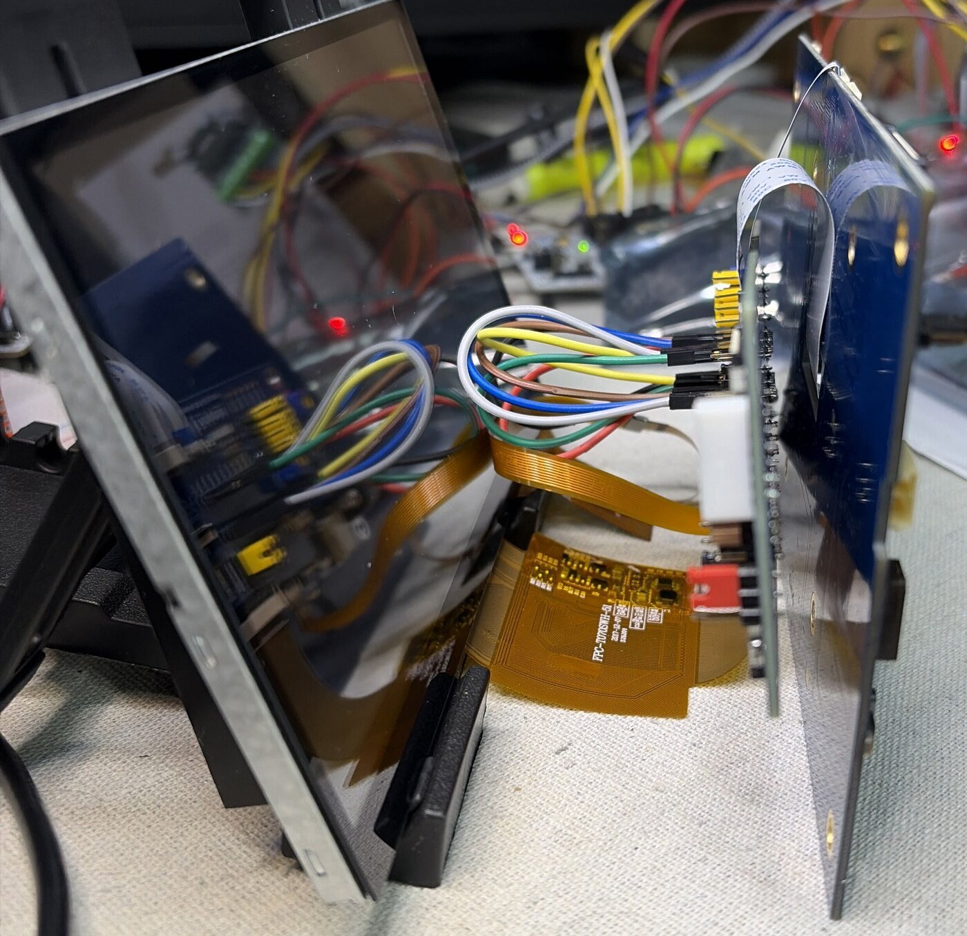
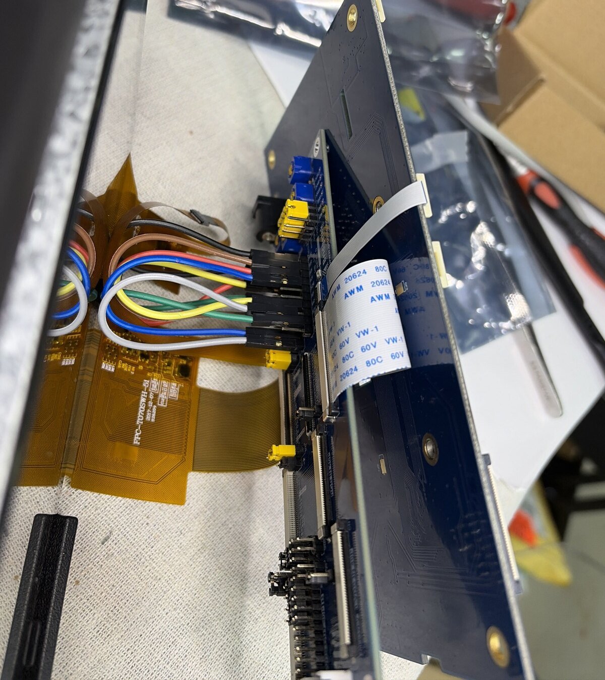
Because of that U-turn in the 50-pin ribbon, the two boards end up folded back to back behind the panel. In my set-up the ME817EV lies against the back of the panel, component side facing away from it, and the adapter folds over behind the ME817EV. The ME817EV has a slot right beside CN2, so on route A the touch extension passes through the board from the panel side and plugs into CN2 from the top. The side view in the route B section below shows the fold.
Pinouts & Configurations
Switch and jumper settings for the PC (USB) host
In this part the PC drives the Bridgetek BT817 through the FT4222H USB bridge on the ME817EV. These are the kit datasheet’s settings for the 7-inch panel, and the ones used for every result in this post:
| Board | Part | Setting | Why |
|---|---|---|---|
| ME817EV | SW1 | Switch 1 ON, switches 2, 3, 4 OFF | Backlight current 160 mA (all OFF is 120 mA; each switch ON adds 40 mA) |
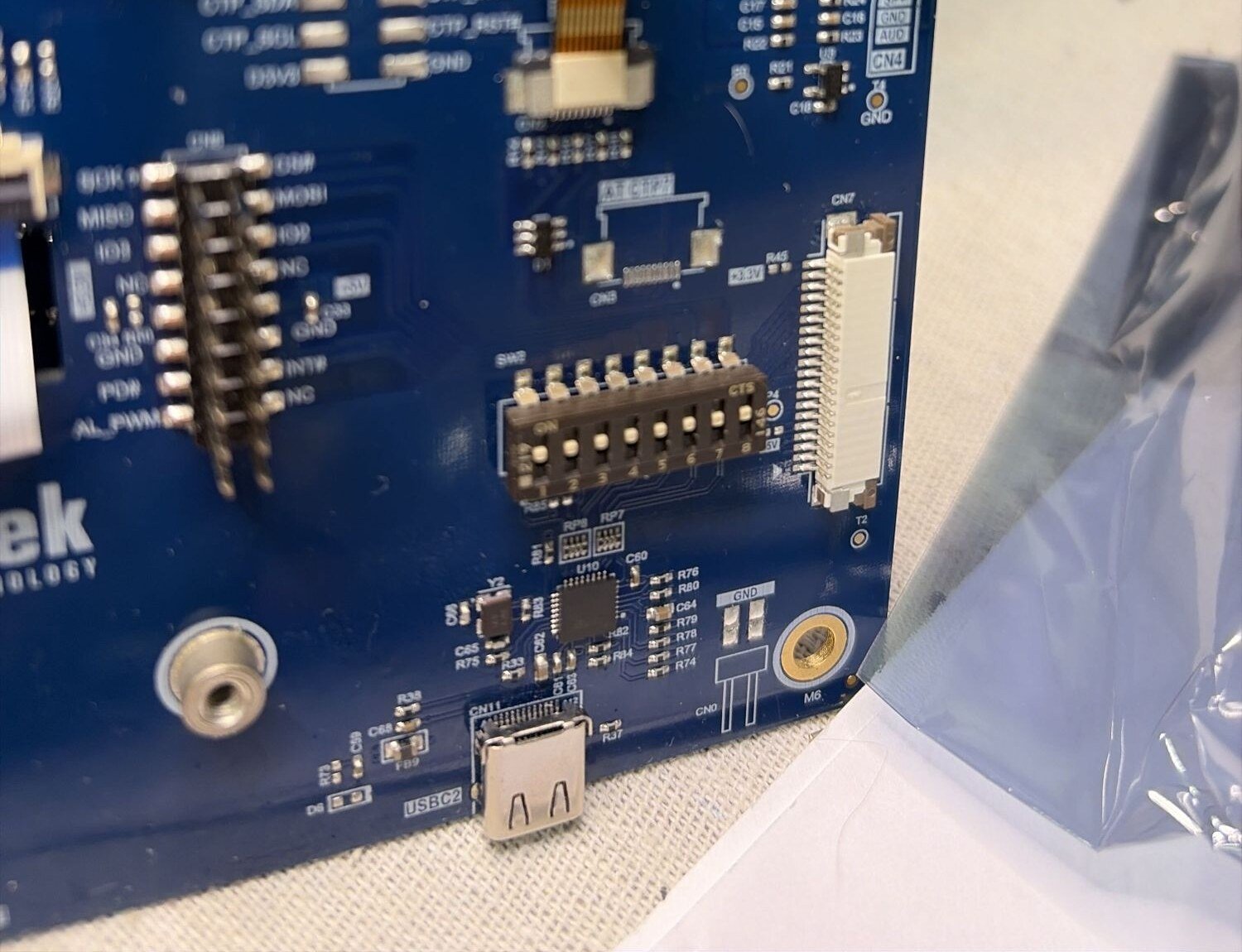
| ME817EV | SW2 | All 8 switches ON | Connects the BT817 host lines to the FT4222H, i.e. to the PC |
| ME817EV | JP1 | Short pins 1-2 | Board power from CN11 (USBC2) |
| VA-1001-01A | JP14, JP16, JP17 | Short pins 2-3 | 3.3 V on the panel’s pins 45, 10 and 9, which this panel needs |
Plug the USB cable into CN11 (USBC2). CN6 (USBC1) also powers the board and the panel lights up, but it has no USB data, so the PC never sees the Bridgetek BT817 kit. When a microcontroller takes over the host lines, SW2 and JP1 change; a future post will cover those settings.
The touch cable: two routes
The panel’s capacitive touch controller (an FT5426) has its own 10-pin flex cable, separate from the display cable. It reaches the Bridgetek BT817 in one of two ways. Both work, and I tested both:
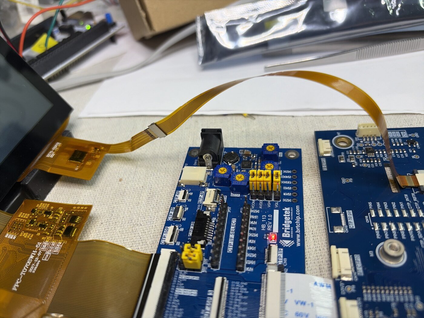
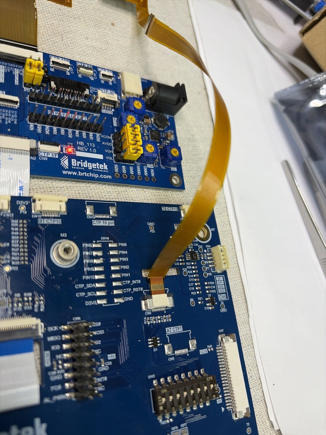
- Route A: panel touch flex → 10-pin extension → ME817EV CN2. No jumpers. This is the route in the kit datasheet.
- Route B: panel touch flex → 10-pin extension → adapter CTP_1 (CTP 10P) → seven jumper wires from JP24 to JP23 (CTP I/F SELECT) → adapter CN9 (CTP I/F) → short white cable → ME817EV CN10 (MT_CTP10). This is the route in Bridgetek’s video.
Use route A with this kit: it is simpler and needs no wiring.
Why are there two routes at all? The answer is in Bridgetek’s own datasheets. The ME817EV is built to work with several Bridgetek panels, so it has several touch sockets, each wired for a different panel’s touch pinout: CN2, CN10 (MT_CTP10), CN12 (AT CTP10), CN14 (TS CTP10), CN15 and CN3 (AT CTP7). This kit’s 7-inch panel has the same pin order as CN2, pin for pin: ground, 3.3 V, SCL, SDA, reset, wake, interrupt, ground. The ME817EV datasheet’s list of tested panels also pairs a 7-inch FT5426 panel with CN2. That is why route A needs nothing between the extension cable and the board.
CN10 is a different story. The same datasheet pairs it with a 10.1-inch LVDS panel that uses a GT928 touch controller, and its pins come in a completely different order: pins 1 to 4 unused, then reset, interrupt, SCL, SDA, ground and 3.3 V. The VA-1001-01A is Bridgetek’s “universal” LCD adapter, meant for panels that fit none of the ME817EV’s sockets. Its JP24 and JP23 headers let you wire any touch pinout across to the order CN10 expects. Route B uses that remapping for a panel that doesn’t need it, which is why it takes seven jumper wires. Bridgetek’s video uses route B for this kit without saying why. My guess is that their demo set-up was simply built around the universal adapter, but nothing in the documents says so.
In both routes the extension cable ends up with a half-twist. The panel’s flex goes into the extension’s socket with its contacts facing up, and the socket’s silver (metal) side also faces up. The kit datasheet says contacts down at this end, which is the opposite. The datasheet’s wording is easy to misread because the socket itself can be held either way up; the photos below show the orientation that works.
Two habits save a lot of time here: unplug the USB cable before reseating any of these cables, and push each flex in until the contacts disappear into the connector before closing its latch. A wrong orientation fails silently: the picture is perfect, but the screen never reacts to a touch. In EVE Screen Designer that looks like a calibration dot that ignores your taps (more on that in the Running It section).
Route A: extension to ME817EV CN2
- Panel touch flex into the extension’s socket: socket silver side up, flex contacts up.
- Other end of the extension into the ME817EV’s CN2 with its contacts facing up (CN2 is a top-contact connector).
Route B: through the adapter, with jumper wires
Before moving the extension, mark its pin-1 edge with a felt-tip pen while it is still in CN2 (pin 1 is the dot beside CN2). Then:
- Extension into the adapter’s CTP_1 (CTP 10P), with the marked edge at the end printed 01.
- Seven female-to-female jumper wires from JP24 to JP23, as in the table below. JP24 pins 4, 6 and 8 stay open.
- The kit’s short white 10-pin cable from the adapter’s CN9 (CTP I/F) to the ME817EV’s CN10 (MT_CTP10). CN10 is a bottom-contact connector, so the cable’s contacts face down there.
| JP24 pin | Panel signal | JP23 pin | JP23 label |
|---|---|---|---|
| 1 | GND | 1 | GND |
| 2 | VDD (3.3 V) | 3 | 3V3 |
| 3 | SCL | 7 | SCL |
| 5 | SDA | 9 | SDA |
| 7 | RST | 2 | RST |
| 9 | INT | 4 | INT |
| 10 | GND | 5 | GND |
JP24 pin 8 is the panel’s WAKE line; touch worked with it left open. The CTP_1 and CN9 connectors have contacts on both sides, so a cable that is in upside down still makes contact, with the pin order reversed. Check the pin-1 mark at each end before powering up.
Route B forces the boards back to back. The white cable from CN9 to CN10 is only a few centimetres long, so the only way to connect them is to fold the adapter upside down behind the ME817EV. Bridgetek’s video shows the jumper wires on the adapter but never mentions them.
Project Setup
Everything in this part runs on a Windows PC. I used Windows 11 in a VirtualBox virtual machine on my Linux desktop and it works fine. If you do the same, pass the kit’s USB device through to the virtual machine. It shows up as FTDI FT4222 (USB ID 0403:601c). A permanent USB filter for that ID makes it attach by itself every time the Bridgetek BT817 kit powers up.
Install EVE Screen Designer
- Download EVE Screen Designer 5.3.0 from brtchip.com/esd.
- Extract the zip and run
EVE Screen Designer.exe. Accept the defaults in the setup wizard and click Install, then Finish. - If Visual Studio 2022 is not on the PC, install the Visual C++ Redistributable for Visual Studio 2022 (x64) from Microsoft. The ESD user guide lists it as a requirement.
- Plug the Bridgetek BT817 kit into the PC (USB-C into CN11). Windows installs the FT4222 driver by itself. In Device Manager it appears as FT4222H Interface A and Interface B.
Your antivirus may stop the first program ESD builds, because it is a brand-new .exe. AVG’s CyberCapture did that on mine. An exception for the ESD projects folder, C:\Users\Public\Documents\EVE Screen Designer\, fixes it.
Create the project
ESD opens with a welcome dialog. Choose Create a new project and pick the IDK-BT817-70A build target. ESD saves the project under C:\Users\Public\Documents\EVE Screen Designer\<project name> and opens it with a first page that holds a “Hello World” label.
Then check the drop-downs in the toolbar, outlined in red below. They tell ESD which hardware to build for:
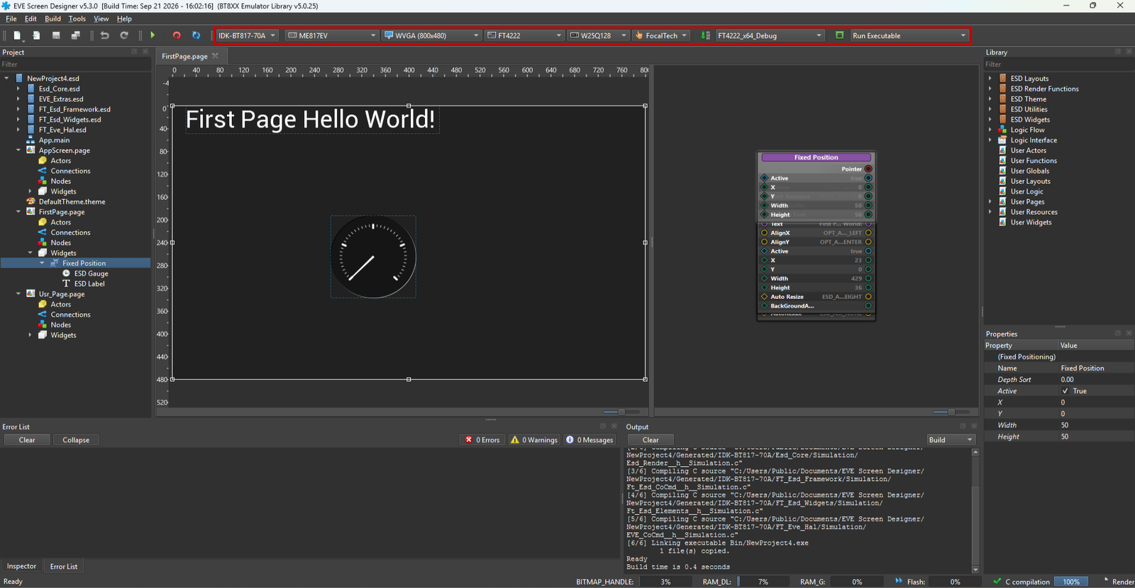
| Drop-down | Setting | Why |
|---|---|---|
| Build target | IDK-BT817-70A | This kit |
| Board | ME817EV | The BT817 board |
| Display | WVGA (800×480) | The 7-inch panel’s resolution |
| Host | FT4222 | The PC talks to the BT817 through the FT4222H USB bridge on the ME817EV |
| Flash | W25Q128 | The 16 MB flash chip on the ME817EV |
| Touch | FocalTech | The panel’s FT5426 is a FocalTech capacitive controller. A resistive setting never registers a tap on this panel. |
| Toolchain | FT4222_x64_Debug | Builds a Windows .exe. The Debug build prints a log to its console window, which is a big help when something goes wrong. |
| Upload mode | Run Executable | Runs the program without rewriting the flash. The other choice, Upload Flash and Run Executable, also writes the project’s images and fonts to the ME817EV’s flash first. |
Watch out for the Touch setting when you open Bridgetek’s example projects. The ones I tried are set up for a kit with a resistive touch panel, so on this kit they sit forever on the first calibration target. Switch them to FocalTech.
If you ever move an ESD project to another folder, copy only the source files, or delete the Build and Cache folders after copying. ESD stores absolute paths in them, and the build fails at the new location until they are regenerated.
Running It on the Hardware
ESD has two ways to run a project, and the toolbar makes them easy to mix up:
- The green Run arrow on the left starts the emulator. The page runs inside ESD on the PC, and the kit does nothing.
- The Build and Upload to Hardware button, just left of the Run Executable drop-down, builds a Windows program and runs it against the real kit through the FT4222.
Use the second one. The Output pane shows the build steps and ends with “Launching: …NewProject4.exe”. A console window then opens with the program’s log:
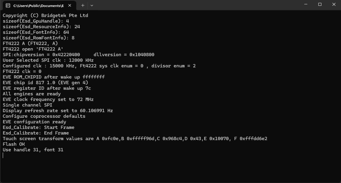
The lines worth reading:
FT4222 open 'FT4222 A': the PC found the kit’s USB bridge.Configured clk : 15000 KHz: ESD asked for 12 MHz SPI and the FT4222 picked its nearest clock, 15 MHz. The link isSingle channel SPI.EVE chip id 817 1.0 (EVE gen 4): the Bridgetek BT817 answered.EVE clock frequency set to 72 MHzandDisplay refresh rate set to 60.106991 Hz: the BT817 is running and driving the panel.Esd_Calibrate: Start Frame…End FrameandTouch screen transform values are ...: touch calibration finished.Flash OK: the on-board flash is attached.
Touch calibration
Before the page appears, the program runs the BT817’s touch calibration. The panel turns light grey and shows a pulsing blue dot. Tap it, and it moves to the next spot. There are three targets in all:
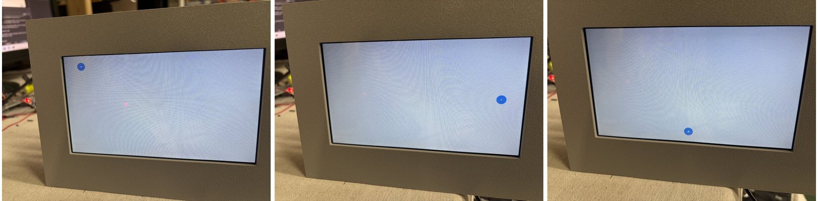
The first time I ran ESD, I took that dot for a loading spinner and waited for it to finish. It’s waiting for you. If tapping it does nothing, the touch signals aren’t reaching the BT817: check the touch cable (see the two routes above) and the FocalTech touch setting. The display side can be perfect while touch is dead, so a good picture doesn’t prove the touch cable is right.
The page on the panel
After the third tap the page from ESD appears on the 7-inch panel. Mine has the label plus a gauge widget:
If nothing happens
Sometimes a hardware run ends with no console window and no message. To see why, open a Command Prompt and run the program yourself. It is in the project folder under Build\IDK-BT817-70A\FT4222_x64_Debug\Bin\. On mine the log said FT_GetDeviceInfoDetail failed, which means the PC could not see the FT4222. That happens when a virtual machine loses the USB device. Unplug the USB-C cable from CN11, wait a few seconds and plug it back in, then run the program again.
Documentation
The Bridgetek documents I used for this part, copied here so the links keep working:
What’s Next
With the kit proven on the PC, a future post will replace the PC with an STM32. A NUCLEO-H753ZI takes over the host lines on the ME817EV’s CN8 header and drives the Bridgetek BT817 over plain SPI, with no EVE Screen Designer in between. That post will cover:
- Wiring CN8 to the Nucleo, with a KiCad schematic of the connections
- The SW2 and JP1 changes for a microcontroller host, and how to power the ME817EV while the Nucleo runs from its ST-LINK
- Waking the BT817, reading its chip ID and putting a first screen on the panel from STM32 code
Later posts will bring touch over to the STM32 with the co-processor’s widgets (buttons, sliders, toggles and dials), draw with the display-list primitives (shapes, colour and alpha, bitmaps), and move the board to QSPI.
If you have questions or run into trouble getting the boards programmed and talking to each other, post in the Tutorial Support forum and I will work through it with you. If project source is not linked in the tutorial, it may be available on request — use the email contact option in the site footer.
Tutorials and code are provided as-is, without warranty. See the Disclaimer.