Overview
This tutorial covers STM32 7-segment display GPIO control using the Output Data Register (ODR) method. You will learn the hardware wiring for a Common Cathode display, CubeMX pin configuration, and the code needed to drive all 7 LED segments. A Common Cathode display turns a segment on when the GPIO pin is High and off when Low — if your supply voltage exceeds 3.3V, use a 220Ω current-limiting resistor on each segment pin.
What You Will Learn
- How to drive a 7 segment display from an STM32 microcontroller
- How to use GPIO output pins and the Output Data Register (ODR)
- How to map display segments to STM32 pins
- How to configure the project in STM32CubeIDE
Prerequisites
Basic familiarity with STM32CubeIDE, embedded C, GPIO concepts, and working with a simple breadboarded hardware setup is recommended.
Materials List
- STM32F103C8TX Be careful when buying cheaper versions to get more boards for less money. They might not be true STM chips and won’t work with STM32CubeIDE. Always look at the label on the CPU make sure you see the STM logo.

- ST-Link V2 Emulator Downloader Programmer
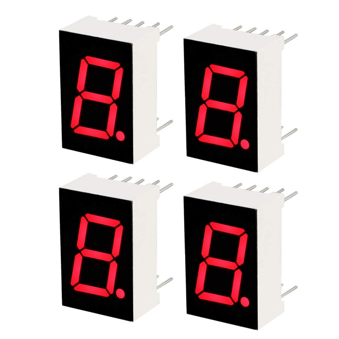
- Common Cathode Blue LED
- Breadboards Kit Include 2PCS 830 Point 2PCS 400 Point Solderless Breadboards
Hardware
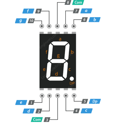
Display Anatomy
You will note that there are 7 segments, plus a decimal point LED, but we won’t be using the decimal point LED known as DP.
Each LED segment is labeled from a-g, with the decimal point LED labeled DP.
Components
This project uses an STM32F103C8TX board, a common cathode 7 segment display, jumper wires, resistors, a breadboard, and an ST-Link programmer.
Schematic
The following is the schematic depicting the wiring needed for this project.

Pinouts
I used a STM32F103C8TX for this project, however any of the STM32 boards will most likely work, including Nucleo boards.
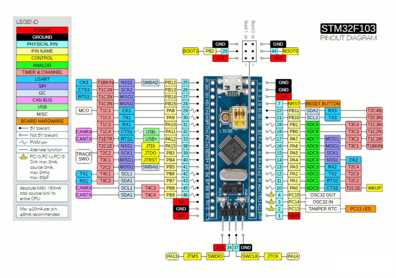
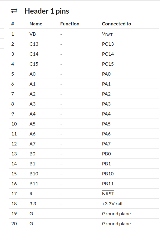
Header 1 Pins
In the diagram above, Header #1 pins are on the right starting from the bottom working upwards. The pin numbers DO NOT match the color coded pin assignment diagram, so count the pins in the below chart upwards from the bottom right side.
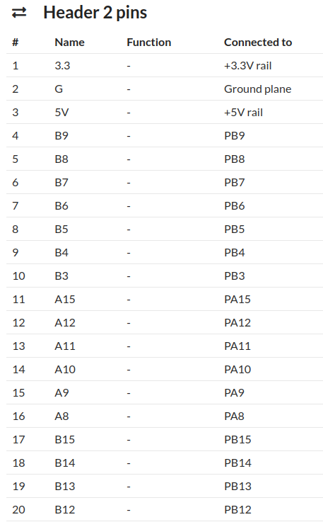
Header 2 Pins
In the diagram above, Header #2 pins start at the bottom left and working upwards. The pin numbers DO NOT match the color coded pin assignment diagram above, so count the pins in the below chart upwards from the bottom left side.
CubeIDE Configuration
We are going to use 7 GPIO pins on Port A out of the 16 total available. We only need 7 because we are controlling a 7 segment display.
After we’ve selected PA0-PA7, as GPIO Output pins your view should look like this. By the way, I didn’t need to select PA7 because we won’t be connecting the decimal point LED, even though I set it up as GPIO Output as well.
Project Setup
Create a new STM32CubeIDE project for the STM32F103C8TX, configure the required GPIO pins on Port A as outputs, generate the code, and then add the display control logic to main.c.
Code Walkthrough
main.c
Below is the code snippet that makes this work. Notice that I’m using binary for a total of 7 bits. Each bit represents a segment on the display.
We are using 7 bits because I’m not using the decimal point LED. Otherwise I’d be using 8 bits.
Using PortX->ODR allows us to set X number of bits on a port up to a maximum of 16 bits. We are only using 7 bits as mentioned above. Setting a bit to 1 turns on the LED segment, and a 0 bit turns it off.
/* Private user code ---------------------------------------------------------*/
/* USER CODE BEGIN 0 */

void delay(uint16_t delay) {
	HAL_Delay(delay);
}

void displayEachSeg() {
		      //      gfedcba
	GPIOA->ODR = 0b00000000;                              //Write to port-A
	delay(1000);
	GPIOA->ODR = 0b00000001;                              //Write to port-A-seg-a
	delay(1000);
	GPIOA->ODR = 0b00000010;                              //Write to port-A-seg-b
	delay(1000);
	GPIOA->ODR = 0b00000100;                              //Write to port-A-seg-c
	delay(1000);
	GPIOA->ODR = 0b00001000;                              //Write to port-A-seg-d
	delay(1000);
	GPIOA->ODR = 0b00010000;                              //Write to port-A-seg-e
	delay(1000);
	GPIOA->ODR = 0b00100000;                              //Write to port-A-seg-f
	delay(1000);
	GPIOA->ODR = 0b01000000;                              //Write to port-A-seg-g
	delay(1000);
	GPIOA->ODR = 0b00000000;                              //Write to port-A-seg-none
	delay(1000);
}

void displayAllSeg() {
		      //      gfedcba
	GPIOA->ODR = 0b00000001;                              //Write to port-A
	delay(1000);
	GPIOA->ODR = 0b00000011;                              //Write to port-A
	delay(1000);
	GPIOA->ODR = 0b00000111;                              //Write to port-A
	delay(1000);
	GPIOA->ODR = 0b00001111;                              //Write to port-A
	delay(1000);
	GPIOA->ODR = 0b00011111;                              //Write to port-A
	delay(1000);
	GPIOA->ODR = 0b00111111;                              //Write to port-A
	delay(1000);
	GPIOA->ODR = 0b01111111;                              //Write to port-A
	delay(1000);
	GPIOA->ODR = 0b00000000;                              //Write to port-A
	delay(1000);
}

void displayZero() {
		      //      gfedcba
	GPIOA->ODR = 0b00111111;                              //Write to port-A
	delay(1000);
}
void displayOne() {
		      //      gfedcba
	GPIOA->ODR = 0b00000110;                              //Write to port-A
	delay(1000);
}

void displayTwo() {
		      //      gfedcba
	GPIOA->ODR = 0b01011011;                              //Write to port-A
	delay(1000);
}

void displayThree() {
		      //      gfedcba
	GPIOA->ODR = 0b01001111;                              //Write to port-A
	delay(1000);
}

void displayFour() {
		      //      gfedcba
	GPIOA->ODR = 0b01100110;                              //Write to port-A
	delay(1000);
}

void displayFive() {
		      //      gfedcba
	GPIOA->ODR = 0b01101101;                              //Write to port-A
	delay(1000);
}

void displaySix() {
		      //      gfedcba
	GPIOA->ODR = 0b01111101;                              //Write to port-A
	delay(1000);
}

void displaySeven() {
		      //      gfedcba
	GPIOA->ODR = 0b00000111;                              //Write to port-A
	delay(1000);
}

void displayEight() {
		      //      gfedcba
	GPIOA->ODR = 0b01111111;                              //Write to port-A
	delay(1000);
}

void displayNine() {
		      //      gfedcba
	GPIOA->ODR = 0b01101111;                              //Write to port-A
	delay(1000);
}

void displayA() {
		      //      gfedcba
	GPIOA->ODR = 0b01110111;                              //Write to port-A
	delay(1000);
}

void displayB() {
		      //      gfedcba
	GPIOA->ODR = 0b01111100;                              //Write to port-A
	delay(1000);
}

void displayC() {
		      //      gfedcba
	GPIOA->ODR = 0b00111001;                              //Write to port-A
	delay(1000);
}

void displayD() {
		      //      gfedcba
	GPIOA->ODR = 0b01011110;                              //Write to port-A
	delay(1000);
}

void displayE() {
		      //      gfedcba
	GPIOA->ODR = 0b01111001;                              //Write to port-A
	delay(1000);
}

void displayF() {
		      //      gfedcba
	GPIOA->ODR = 0b01110001;                              //Write to port-A
	delay(1000);
}

/* USER CODE END 0 */

/**
  * @brief  The application entry point.
  * @retval int
  */
int main(void)
{

  /* USER CODE BEGIN 1 */

  /* USER CODE END 1 */

  /* MCU Configuration--------------------------------------------------------*/

  /* Reset of all peripherals, Initializes the Flash interface and the Systick. */
  HAL_Init();

  /* USER CODE BEGIN Init */

  /* USER CODE END Init */

  /* Configure the system clock */
  SystemClock_Config();

  /* USER CODE BEGIN SysInit */

  /* USER CODE END SysInit */

  /* Initialize all configured peripherals */
  MX_GPIO_Init();
  /* USER CODE BEGIN 2 */

  /* USER CODE END 2 */

  /* Infinite loop */
  /* USER CODE BEGIN WHILE */
  while (1)
  {
    /* USER CODE END WHILE */
    /* USER CODE BEGIN 3 */
	  displayEachSeg();
	  displayAllSeg();
    displayZero();
	  displayOne();
	  displayTwo();
	  displayThree();
	  displayFour();
	  displayFive();
	  displaySix();
	  displaySeven();
	  displayEight();
	  displayNine();
	  displayA();
	  displayB();
	  displayC();
	  displayD();
	  displayE();
	  displayF();
  }
  /* USER CODE END 3 */
}

/**
  * @brief GPIO Initialization Function
  * @param None
  * @retval None
  */
static void MX_GPIO_Init(void)
{
  GPIO_InitTypeDef GPIO_InitStruct = {0};
/* USER CODE BEGIN MX_GPIO_Init_1 */
/* USER CODE END MX_GPIO_Init_1 */

  /* GPIO Ports Clock Enable */
  __HAL_RCC_GPIOA_CLK_ENABLE();

  /*Configure GPIO pin Output Level */
  HAL_GPIO_WritePin(GPIOA, GPIO_PIN_0|GPIO_PIN_1|GPIO_PIN_2|GPIO_PIN_3
                          |GPIO_PIN_4|GPIO_PIN_5|GPIO_PIN_6|GPIO_PIN_7, GPIO_PIN_RESET);

  /*Configure GPIO pins : PA0 PA1 PA2 PA3
                           PA4 PA5 PA6 PA7 */
  GPIO_InitStruct.Pin = GPIO_PIN_0|GPIO_PIN_1|GPIO_PIN_2|GPIO_PIN_3
                          |GPIO_PIN_4|GPIO_PIN_5|GPIO_PIN_6|GPIO_PIN_7;
  GPIO_InitStruct.Mode = GPIO_MODE_OUTPUT_PP;
  GPIO_InitStruct.Pull = GPIO_NOPULL;
  GPIO_InitStruct.Speed = GPIO_SPEED_FREQ_LOW;
  HAL_GPIO_Init(GPIOA, &GPIO_InitStruct);

/* USER CODE BEGIN MX_GPIO_Init_2 */
/* USER CODE END MX_GPIO_Init_2 */
}
If you have questions or run into trouble getting the boards programmed and talking to each other, post in the Tutorial Support forum and I will work through it with you. If project source is not linked in the tutorial, it may be available on request — use the email contact option in the site footer.