Overview
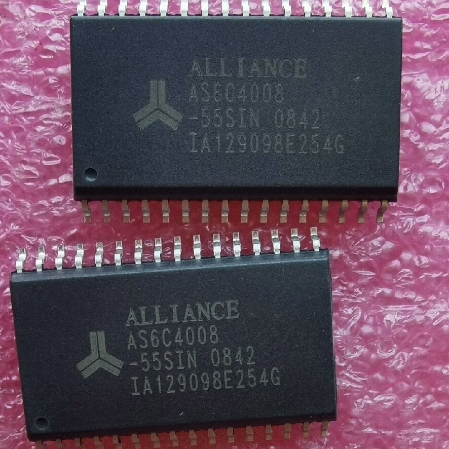
In this tutorial, you will learn how to interface external SRAM with STM32H753 using the Flexible Memory Controller (FMC). This STM32H753 external SRAM project uses an AS6C4008 512 KB asynchronous SRAM device connected through a custom FMC daughterboard.
If you are new to external SRAM on STM32 microcontrollers, I recommend starting with my STM32F439 External SRAM Setup and Code Walkthrough tutorial. That article covers the original AS6C4008 SRAM daughterboard design, FMC fundamentals, hardware connections, and the initial validation methodology. This STM32H753 tutorial builds upon that foundation and focuses on the Cortex-M7-specific considerations encountered while porting the project to the STM32H753ZI.
The goal of this project is not only to connect external memory, but to fully validate the SRAM hardware, integrate it into the STM32H753 memory map, place initialized data into external SRAM with a linker section, and document the Cortex-M7-specific MPU configuration required for reliable operation.
This article builds on the earlier STM32F439 external SRAM tutorial. The F439 version covers the original daughterboard design, AS6C4008 hardware overview, FMC fundamentals, and basic validation strategy. This STM32H753 version focuses on the H753 port, including FMC_NE1 pin mapping, linker integration, startup-copy support, MPU configuration, debugging, and final validation testing.
The most important lesson from the STM32H753 port is that a design which works correctly on the STM32F439 does not automatically behave the same way on the Cortex-M7 based STM32H753. The H753 implementation initially showed SRAM corruption in structures, strings, floating-point values, and initialized application data until the FMC SRAM region at 0x60000000 was configured through the MPU before HAL_Init().
- Overview
- What You Will Learn
- Prerequisites
- Materials List
- Reference: Original STM32F439ZI Tutorial
- Porting from STM32F439ZI to STM32H753ZI
- Project Structure
- Hardware Configuration / Pinouts
- Project Setup
- FMC Configuration
- FMC_NE1 Pin-Mapping Correction
- Code Walkthrough
- Debugging the H753 Port
- Root Cause Analysis
- Final Validated Configuration
- Test Results
- Project Downloads
- Documentation
- Conclusion
What You Will Learn
- How to configure FMC external SRAM on the STM32H753ZI
- How the AS6C4008 SRAM daughterboard maps into the STM32 address space
- How to preserve the F439 daughterboard signal mapping while porting to H753
- How to add an external SRAM region to the H753 linker script
- How to copy initialized
.sramdatacontents from FLASH into external SRAM - Why Cortex-M7 MPU configuration is required for reliable FMC SRAM access
- How to validate the full 512 KB SRAM region using structured tests
Prerequisites
This tutorial assumes that you are already comfortable with STM32CubeIDE, STM32CubeMX, embedded C, basic linker-script editing, and normal STM32 project generation. It also assumes that you understand the basic FMC SRAM concept from the earlier STM32F439ZI tutorial.
If you have not already reviewed the STM32F439ZI SRAM daughterboard tutorial, start there first for the broader hardware background, AS6C4008 overview, and FMC fundamentals. This STM32H753 external SRAM article focuses on the porting details and the Cortex-M7-specific behavior.
Materials List
- STM32 Nucleo-H753ZI development board
- Custom AS6C4008 FMC SRAM daughterboard
- USB cable for programming and serial output
- STM32CubeIDE
- STM32CubeMX 6.14.1
- STM32Cube FW_H7 V1.12.1
- Optional: logic analyzer for FMC signal validation
- Optional: Doxygen for generated project documentation
Reference: Original STM32F439ZI Tutorial
This project reuses the same AS6C4008 SRAM daughterboard concept from the STM32F439ZI tutorial. The F439 article remains the best place to cover the original daughterboard design, general FMC concepts, AS6C4008 hardware overview, and the initial validation philosophy.
The H753 version should not be treated as a duplicate of the F439 article. Instead, this article documents what changed when the same external SRAM design was ported from a Cortex-M4 STM32F439ZI to a Cortex-M7 STM32H753ZI.
STM32F439 External SRAM Setup and Code Walkthrough
Porting from STM32F439ZI to STM32H753ZI
The most important part of this project was not simply enabling FMC on another STM32 board. The original STM32F439 external SRAM project already proved that the AS6C4008 daughterboard design worked. The H753 project was a port of that working design to a different STM32 family, and the differences between the STM32F439ZI and STM32H753ZI mattered.
At the board level, the external SRAM daughterboard was still reusable. The AS6C4008 device, address bus, data bus, and core FMC memory-mapped access model remained the same. From the firmware point of view, the external SRAM was still intended to appear at 0x60000000 and be accessed using normal pointer reads and writes.
The major differences were not in the SRAM chip itself. They came from the STM32H753 platform: the Cortex-M7 core, the H7 memory system, the CubeMX pin-selection behavior, and the need to explicitly configure the external SRAM region through the MPU.
F439 Baseline
The original STM32F439ZI implementation used a Cortex-M4 core. In that project, the FMC SRAM region worked correctly using the default memory attributes. No explicit MPU configuration was required for the external SRAM daughterboard to operate correctly.
That F439 baseline was important because it proved the daughterboard concept, the AS6C4008 wiring, the FMC memory window, the validation approach, the linker-section approach, and the startup-copy approach. When the same concept was moved to the H753, the expectation was that most of the hardware model would remain valid.
H753 Platform Differences
The STM32H753ZI uses a Cortex-M7 core with a more advanced memory subsystem. Compared with the STM32F439ZI, the H753 can involve caching, buffering, and memory-access behavior that must be controlled more carefully when using external asynchronous memory.
That distinction became the central lesson of the port. The external SRAM could appear to work during simple tests, yet still corrupt structured application data when the memory region was left with unsuitable default attributes.
| Topic | STM32F439ZI Project | STM32H753ZI Project |
|---|---|---|
| CPU core | Cortex-M4 | Cortex-M7 |
| External SRAM device | AS6C4008, 512 KB | AS6C4008, 512 KB |
| FMC SRAM base address | 0x60000000 | 0x60000000 |
| FMC_NE1 target pin | PD7 | PC7->PD7 after correction |
| MPU requirement | Not required for this project | Required before HAL_Init() |
| Observed failure without MPU fix | Not observed | Structured SRAM corruption |
| Final validation | SRAM tests passed | Integration tests and full 512 KB pattern tests passed |
FMC_NE1 Pin Mapping Difference
One subtle but important porting issue involved the FMC_NE1 chip-select signal. The original STM32F439ZI project used PD7 for FMC_NE1, and the SRAM daughterboard routing was built around that assignment.
During the initial STM32H753ZI CubeMX configuration, FMC_NE1 was automatically assigned to PC7, which is also a valid alternate-function pin for the H753 FMC peripheral. Although electrically valid for a new design, that assignment did not match the existing daughterboard wiring. To preserve compatibility with the original hardware, the H753 configuration was modified so that FMC_NE1 was moved from PC7 back to PD7. This allowed the same AS6C4008 SRAM daughterboard to be reused without any PCB changes.
The final validated STM32H753ZI configuration therefore used FMC_NE1 on PD7, matching the original STM32F439ZI hardware design and preserving compatibility with the existing AS6C4008 SRAM daughterboard.
This is an important distinction: the final H753 design did not require a new SRAM daughterboard. It required the H753 FMC pin configuration to be aligned with the existing daughterboard wiring.
| Signal | STM32F439ZI Design Intent | Final STM32H753ZI Configuration | Reason It Matters |
|---|---|---|---|
FMC_NE1 | PD7 | PC7->PD7 | Preserves daughterboard chip-select routing |
FMC_NOE | FMC output enable | PD4 | Controls SRAM read cycles |
FMC_NWE | FMC write enable | PD5 | Controls SRAM write cycles |
FMC_D0-D7 | 8-bit SRAM data bus | PD14, PD15, PD0, PD1, PE7-PE10 | Provides byte-wide SRAM data access |
FMC_A0-A18 | 19-bit SRAM address bus | PF0-PF5, PF12-PF15, PG0-PG5, PD11-PD13 | Addresses the full 512 KB SRAM device |
Why the Pin Mapping Issue Was Separate from the MPU Issue
The FMC_NE1 correction was a hardware-configuration alignment issue. The MPU fix was a Cortex-M7 memory-system issue. They were related only because both had to be correct before the H753 project could be considered fully validated.
If FMC_NE1 is wrong, the SRAM chip-select path does not match the daughterboard wiring. The external SRAM may not respond correctly because the hardware is not being selected as intended.
If the MPU configuration is missing, the SRAM can still appear to respond, but structured data can become corrupted because the Cortex-M7 memory system is using inappropriate attributes for the external asynchronous SRAM window.
That is why this port required both checks: first confirm that the H753 FMC pins match the daughterboard wiring, then confirm that the Cortex-M7 MPU attributes match the behavior required by the external SRAM memory region.
Failure Signature Seen During the H753 Port
Before the MPU region was configured correctly, the H753 project showed a specific kind of failure. Simple SRAM access could look plausible, but structured data operations exposed corruption.
- Structure fields did not always retain the expected values.
- String writes could affect nearby structure fields.
- Floating-point fields could become corrupted.
- Array updates could disturb data outside the intended field boundaries.
- Basic raw memory tests were not sufficient by themselves to prove full correctness.
That failure pattern is why the integration test became so useful. The test did not only write raw bytes into SRAM. It placed a structured object into the external SRAM section and then verified strings, floats, integer fields, array contents, and sentinel values before and after modification.
Final H753 Porting Rule
The final design rule from the port is straightforward: when using FMC external SRAM on the STM32H753, configure the external SRAM region through the MPU before HAL_Init().
- Base address:
0x60000000 - Region size:
MPU_REGION_SIZE_512KB - Cacheable: no
- Bufferable: no
- Shareable: yes
- Execute permission: execute-never
Project Structure
Core/
├── Inc/
│   ├── main.h
│   ├── sram_integration.h
│   └── sram_validation.h
├── Src/
│   ├── main.c
│   ├── globalDataCopy.s
│   ├── sram_integration.c
│   ├── sram_validation.c
│   ├── 00_sram_architecture_overview.dox
│   ├── 01_sram_docs_index.dox
│   ├── 02_sram_validation_tests.dox
│   ├── 03_sram_integration_flow.dox
│   ├── 04_h753_porting_notes.dox
│   ├── 05_h753_memory_map_and_linker.dox
│   └── 07_h753_flash_linker_script_reference.dox
STM32H753ZITX_FLASH.ld
H753_CPP_AS6C4008_FMC_DaughterBoard_02.pdf
Hardware Configuration / Pinouts
Overview
The hardware arrangement is the same basic architecture as the STM32F439ZI project: the Nucleo board provides the MCU and FMC peripheral, while the AS6C4008 daughterboard provides the external asynchronous SRAM device and the routing between the SRAM and the Nucleo Morpho headers.
From the firmware perspective, the SRAM is not accessed through SPI, I2C, or a command protocol. Once FMC is initialized, the SRAM appears as a memory-mapped region beginning at 0x60000000. Normal pointer reads and writes become FMC bus cycles.
PCB Overview
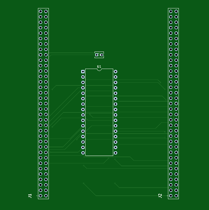
This PCB hosts the AS6C4008 SRAM and routes the FMC address, data, and control signals from the STM32H753. The wide parallel traces at the bottom of the board correspond to the address and data buses.
The PCB is designed as a daughterboard that plugs directly into the STM32 Nucleo-H753 through the two Morpho expansion connectors. Those connectors expose the STM32H753’s FMC-related GPIO signals, allowing the microcontroller to drive an external parallel SRAM device through the board-to-board connection rather than through flying wires or a separate cable harness.
On the SRAM board, two 70-pin female headers mate with the Nucleo-H753 Morpho headers. When the daughterboard is installed, the FMC address bus, data bus, and control lines are carried from the Nucleo into the SRAM PCB through those connectors. In other words, the Nucleo board is the active controller, and the daughterboard is the memory expansion hardware attached to it.
From the software point of view, the firmware does not communicate with the SRAM board using a serial protocol such as SPI or I2C. Instead, once the FMC peripheral is configured correctly, the external SRAM appears as a memory-mapped region in the STM32 address space starting at 0x60000000. Reads and writes are then performed using normal pointer-based memory access, while the FMC hardware automatically drives the necessary external bus timing over the Morpho connector pins.
This physical and logical arrangement is one of the main strengths of the design. The PCB provides the electrical routing and SRAM device, the Nucleo provides the MCU and FMC peripheral, and the Morpho connectors form the bridge between them. That makes it possible to validate the SRAM hardware, place selected data into external memory, and treat the daughterboard as a true memory expansion platform for the STM32F439.
Schematic

Pinouts & Configuration
The H753 CubeMX IOC export confirms the FMC signal assignment used by the validated project. The most important porting detail is that FMC_NE1 was corrected to PD7, matching the original F439 daughterboard expectation.
FMC_NE1  PD7
FMC_NOE  PD4
FMC_NWE  PD5

FMC_A0   PF0
FMC_A1   PF1
FMC_A2   PF2
FMC_A3   PF3
FMC_A4   PF4
FMC_A5   PF5
FMC_A6   PF12
FMC_A7   PF13
FMC_A8   PF14
FMC_A9   PF15
FMC_A10  PG0
FMC_A11  PG1
FMC_A12  PG2
FMC_A13  PG3
FMC_A14  PG4
FMC_A15  PG5
FMC_A16  PD11
FMC_A17  PD12
FMC_A18  PD13

FMC_D0   PD14
FMC_D1   PD15
FMC_D2   PD0
FMC_D3   PD1
FMC_D4   PE7
FMC_D5   PE8
FMC_D6   PE9
FMC_D7   PE10

USART1_TX  PA9
USART1_RX PA10Project Setup
Create a new STM32CubeIDE project targeting the STM32H753ZI. Enable FMC in CubeMX for asynchronous SRAM on Bank 1 / NE1, configure an 8-bit data bus, and enable the address lines required for the 512 KB AS6C4008 SRAM.
The validated project uses USART1 for console output. This makes it possible to view the integration tests, validation test progress, and final PASS/FAIL status in a serial terminal.
FMC Configuration
The FMC configuration initializes Bank 1 as asynchronous SRAM with an 8-bit data bus. The external SRAM still depends on the FMC timing and GPIO configuration, but on the H753 that is not enough by itself. Correct structured operation also depends on the MPU configuration shown later.
hsram1.Instance = FMC_NORSRAM_DEVICE;
hsram1.Extended = FMC_NORSRAM_EXTENDED_DEVICE;

hsram1.Init.NSBank = FMC_NORSRAM_BANK1;
hsram1.Init.DataAddressMux = FMC_DATA_ADDRESS_MUX_DISABLE;
hsram1.Init.MemoryType = FMC_MEMORY_TYPE_SRAM;
hsram1.Init.MemoryDataWidth = FMC_NORSRAM_MEM_BUS_WIDTH_8;
hsram1.Init.BurstAccessMode = FMC_BURST_ACCESS_MODE_DISABLE;
hsram1.Init.WriteOperation = FMC_WRITE_OPERATION_ENABLE;
hsram1.Init.WaitSignal = FMC_WAIT_SIGNAL_DISABLE;
hsram1.Init.ExtendedMode = FMC_EXTENDED_MODE_DISABLE;
hsram1.Init.AsynchronousWait = FMC_ASYNCHRONOUS_WAIT_DISABLE;
hsram1.Init.WriteBurst = FMC_WRITE_BURST_DISABLE;
hsram1.Init.ContinuousClock = FMC_CONTINUOUS_CLOCK_SYNC_ONLY;
hsram1.Init.WriteFifo = FMC_WRITE_FIFO_DISABLE;
hsram1.Init.PageSize = FMC_PAGE_SIZE_NONE;

Timing.AddressSetupTime = 4;
Timing.AddressHoldTime = 15;
Timing.DataSetupTime = 10;
Timing.BusTurnAroundDuration = 1;
Timing.CLKDivision = 16;
Timing.DataLatency = 17;
Timing.AccessMode = FMC_ACCESS_MODE_A;FMC_NE1 Pin-Mapping Correction
The earlier porting section explains why FMC_NE1 mattered. In the final validated H753 configuration, FMC_NE1 is assigned to PD7, matching the original F439 daughterboard routing.
This correction is worth calling out separately because it is easy to assume that CubeMX-selected FMC pins automatically match an existing daughterboard. In this project, the daughterboard already defined the expected chip-select route, so the H753 CubeMX configuration had to be corrected to match the hardware.
FMC_NE1 = PD7Code Walkthrough
The code is divided into four main pieces: FMC initialization, linker placement, startup relocation, and validation. The critical H753-specific addition is the MPU configuration that must run before HAL_Init().
MPU Configuration
This is the most important H753-specific code in the project. The SRAM region begins at 0x60000000 and is configured as a 512 KB MPU region. The region is non-cacheable, non-bufferable, shareable, and execute-never.
The function must execute before HAL_Init(). That ordering ensures the memory attributes are correct before the HAL and application begin using the memory system.
static void MPU_Config(void)
{
  MPU_Region_InitTypeDef mpuInitStruct = {0};

  HAL_MPU_Disable();

  mpuInitStruct.Enable = MPU_REGION_ENABLE;
  mpuInitStruct.Number = MPU_REGION_NUMBER0;
  mpuInitStruct.BaseAddress = SRAM_BANK_ADDR;
  mpuInitStruct.Size = MPU_REGION_SIZE_512KB;
  mpuInitStruct.SubRegionDisable = 0x00U;
  mpuInitStruct.TypeExtField = MPU_TEX_LEVEL0;
  mpuInitStruct.AccessPermission = MPU_REGION_FULL_ACCESS;
  mpuInitStruct.DisableExec = MPU_INSTRUCTION_ACCESS_DISABLE;
  mpuInitStruct.IsShareable = MPU_ACCESS_SHAREABLE;
  mpuInitStruct.IsCacheable = MPU_ACCESS_NOT_CACHEABLE;
  mpuInitStruct.IsBufferable = MPU_ACCESS_NOT_BUFFERABLE;

  HAL_MPU_ConfigRegion(&mpuInitStruct);
  HAL_MPU_Enable(MPU_PRIVILEGED_DEFAULT);
}Main Initialization Order
The final startup order is intentional. The MPU is configured first, then HAL initialization runs, then clocks and peripherals are initialized, then the custom SRAM startup copy runs.
int main(void)
{
  /* USER CODE BEGIN 1 */
  MPU_Config();
  /* USER CODE END 1 */

  HAL_Init();

  SystemClock_Config();

  MX_GPIO_Init();
  MX_USART1_UART_Init();
  MX_FMC_Init();

  printf("\x1b[2J\x1b[H");
  printf("==============================================================================\r\n");

  globalDataCopy();

#ifdef SRAM_INTEGRATION_TEST_ENABLE
  SramIntegration_RunStructTest();
  SramIntegration_RunStructRawDumpTest();
#else
  gSramValidationReport = SramValidation_RunAll();
#endif

  while (1)
  {
  }
}Linker Script (.sramdata section)
The linker script adds an external SRAM memory region at 0x60000000 and defines a custom .sramdata output section. Initialized variables placed in this section live in external SRAM at runtime, while their initial values are stored in the FLASH image.
MEMORY
{
  FLASH (rx)     : ORIGIN = 0x08000000, LENGTH = 2048K
  DTCMRAM (xrw)  : ORIGIN = 0x20000000, LENGTH = 128K
  RAM_D1 (xrw)   : ORIGIN = 0x24000000, LENGTH = 512K
  RAM_D2 (xrw)   : ORIGIN = 0x30000000, LENGTH = 288K
  RAM_D3 (xrw)   : ORIGIN = 0x38000000, LENGTH = 64K
  ITCMRAM (xrw)  : ORIGIN = 0x00000000, LENGTH = 64K

  /* External SRAM region mapped through FMC Bank1. */
  SRAM (rw)      : ORIGIN = 0x60000000, LENGTH = 512K
}

_sisram = LOADADDR(.sramdata);

.sramdata :
{
  . = ALIGN(4);
  _ssramdata = .;
  *(.sramdata)
  *(.sramdata*)

  . = ALIGN(4);
  _esramdata = .;
} > SRAM AT> FLASHStartup Copy Routine (globalDataCopy.s)
The startup copy helper copies the initialized .sramdata payload from FLASH into external SRAM. This is separate from the normal STM32 startup copy of the internal .data section.
/*
 * @file globalDataCopy.s
 * @ingroup SRAMIntegrationLayer
 * @brief Copies initialized .sramdata contents from FLASH into external SRAM.
 */

.syntax unified
.cpu cortex-m4
.text
  .thumb

     .global  globalDataCopy
     .p2align 2
     .type    globalDataCopy,%function

globalDataCopy:
     .fnstart

      ldr r0, =_ssramdata
      ldr r1, =_esramdata
      ldr r2, =_sisram
      movs r3, #0
      b LoopCopyDataInit

CopyDataInit:
      ldr r4, [r2, r3]
      str r4, [r0, r3]
      adds r3, r3, #4

LoopCopyDataInit:
      adds r4, r0, r3
      cmp r4, r1
      bcc CopyDataInit

      bx lr
.fnendPlacing Initialized Data in External SRAM
The project uses a small SRAM macro to place selected objects into the custom linker section. This keeps SRAM usage explicit. Only variables marked with this attribute are moved into the external SRAM runtime section.
#define SRAM __attribute__((section(".sramdata")))

typedef struct {
  int table[5];
} arrayTest_t;

typedef struct {
  int test1;
  char buf[100];
  float myFloat;
  arrayTest_t myArray;
  int test2;
} FRAM_t;

static SRAM FRAM_t testStruct = {
  .test1 = 100,
  .buf = "This is a test",
  .myFloat = 3.1415f,
  .myArray = { .table = {200, 0, 0, 0, 0} },
  .test2 = 10
};Validation Framework
The validation layer tests the SRAM address range directly and keeps the report structure in internal MCU RAM. This avoids trusting the external SRAM to hold the test result while the external SRAM itself is being validated.
#define SRAM_VALIDATION_BASE_ADDR         ((uint32_t)0x60000000u)
#define SRAM_VALIDATION_TOTAL_SIZE_BYTES  ((uint32_t)(512u * 1024u))
#define SRAM_VALIDATION_SMALL_RANGE_SIZE  ((uint32_t)256u)
#define SRAM_VALIDATION_PATTERN_TEST_SIZE ((uint32_t)(8u * 1024u))
#define SRAM_VALIDATION_ALIAS_COUNT       ((uint32_t)19u)

typedef struct {
  sramValidationStatus_t status;
  sramValidationTestId_t failedTest;
  sramValidationPhase_t failedPhase;
  uint32_t failedOffset;
  uint8_t expectedValue;
  uint8_t actualValue;
  uint32_t testsRun;
} sramValidationReport_t;

const sramValidationReport_t *SramValidation_RunAll(void);
const sramValidationReport_t *SramValidation_GetReport(void);
HAL_StatusTypeDef SramValidation_RunPatternTest(void);Debugging the H753 Port
The H753 port did not fail in an obvious way. The FMC peripheral initialized, basic memory access appeared to work, and simple tests could suggest that the hardware was correct. The failures became obvious when initialized structures, strings, floating-point values, and arrays were placed into external SRAM.
The most important observation was that the failures affected structured application data more than simple byte-level access. That shifted the investigation away from a simple wiring failure and toward memory attributes, bus behavior, and Cortex-M7-specific memory-system behavior.
Root Cause Analysis
The original STM32F439ZI project used a Cortex-M4 core and worked without any explicit MPU configuration for the FMC SRAM region. The STM32H753ZI uses a Cortex-M7 core, and the memory system is more complex.
On the H753, the external SRAM region must be explicitly described to the MPU. Without that region, the CPU can use memory attributes that are inappropriate for asynchronous external SRAM. The resulting behavior can look like data corruption even when the FMC bus and SRAM hardware are otherwise functioning.
The final diagnosis was that the SRAM at 0x60000000 needed to be configured as non-cacheable, non-bufferable, shareable, and execute-never before HAL_Init().
Final Validated Configuration
- Base address:
0x60000000 - SRAM size: 512 KB
- FMC bank: Bank 1 / NE1
- FMC_NE1 pin: PD7
- Data width: 8 bits
- Address lines: A0 through A18
- MPU region size: 512 KB
- MPU cacheable: no
- MPU bufferable: no
- MPU shareable: yes
- MPU execute permission: execute-never
- MPU setup location: before
HAL_Init()
Test Results
For details on testing and how to perform validation, please refer back to the tutorial: STM32F439 External SRAM Setup and Code Walkthrough
Project Downloads
The complete project source code used in this tutorial is available for download. This includes the STM32CubeIDE project files, source code, linker script, startup copy helper, validation modules, and Doxygen documentation sources.
- Full STM32CubeIDE Project (Source + Configuration)
- Doxygen Documentation Package
- H753 IOC / CubeMX Configuration Report
- Generated H753 Project PDF Documentation
Documentation
This project includes Doxygen-generated documentation for the SRAM subsystem, validation layer, integration flow, H753 porting notes, memory map, linker script reference, and MPU design notes.
After downloading the documentation package, open the generated documentation locally by launching:
H753_CPP_AS6C4008_FMC_DaughterBoard_02/docs/html/index.htmlThe documentation is intended to complement this tutorial. The tutorial explains the project flow and the H753 bring-up narrative, while the Doxygen output provides detailed source-level reference material.
Conclusion
The STM32H753ZI FMC SRAM daughterboard port showed that a design which works on the STM32F439ZI does not necessarily transfer unchanged to a Cortex-M7 device. The hardware and FMC concepts remained familiar, but the H753 memory system introduced an additional requirement: the external SRAM region must be configured correctly through the MPU.
Once the FMC_NE1 mapping was corrected, the linker and startup-copy flow were in place, and the MPU region was configured before HAL_Init(), the AS6C4008 external SRAM operated reliably. The final project passed both structured integration tests and full 512 KB validation testing.
The key lesson is simple: on STM32H7/Cortex-M7 systems, external memory validation is not only a hardware or FMC timing problem. MPU memory attributes are part of the hardware bring-up checklist.
If you have questions or run into trouble getting the boards programmed and talking to each other, post in the Tutorial Support forum and I will work through it with you. If project source is not linked in the tutorial, it may be available on request — use the email contact option in the site footer.